
TSMC to Begin 5nm Production While Unveiling Plans for 3nm Technology
Last updated September 23, 2021
- TSMC will begin mass-producing 5 nm chips by April this year, joining Samsung in the category.
- Both have plans for 3 nm semiconductors too, which we will hopefully see in prototypes by 2021.
- The thriving 7 nm will become more mainstream in the next two years, as its cost will drop.
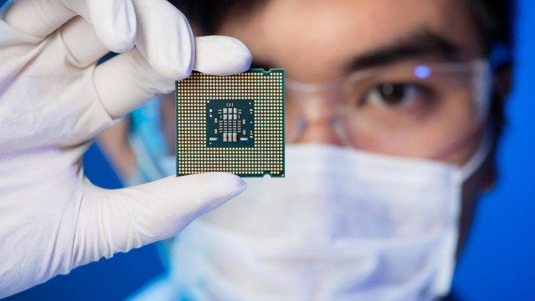
TSMC (Taiwan Semiconductor Manufacturing Company) is making a big step forward by announcing that their readiness to begin mass-producing 5 nm chips. Reportedly, the first chips of this kind will start leaving the production lines of the successful chip maker by April 2020, unless the dramatic situation with Covid-19 that has placed the whole world on pause changes something. The chips will be made using the ultraviolet lithography process technology and will be the penultimate optimization step of the 7LPP tech.
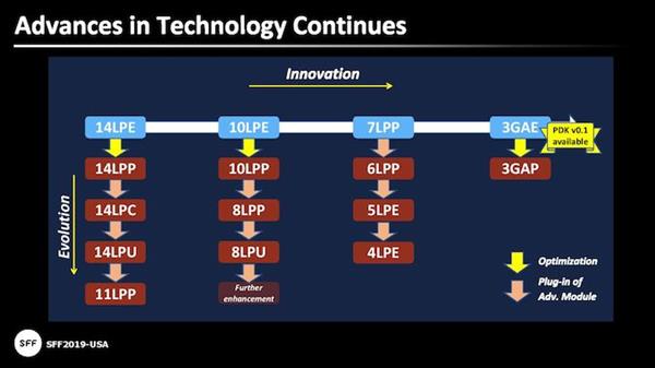
In regards to the “mature” 7 nm node, which is what the chips of current flagships were created on, their production will continue throughout the year and is expected to enjoy the lion’s share in the company’s revenues. Essentially, better yields will result in broader availability, which will bring 7 nm chips down to the mid-range device market. Smaller node means increased transistor density, more powerful processors for the same volume, reduced energy consumption, and thus better battery life. So, the chip makers are striving to shrink transistors inside chips as much as possible. Still, limitations induced by our knowledge in quantum physics have made this scaling down increasingly harder.
We’re moving forward, though, with innovators like TSMC and Samsung leading the race. iPhone 12’s A14 Bionic will be made by TSMC on 5nm lithography, while Samsung Electronics was the first to make the leap, by offering 5 nm chips to its customers by the end of 2018. The same two players are now unveiling the first details about the next step, which will be the 3-nanometer nodes. TSMC announced that it had invested $19.5 billion in the construction of a new 3 nm factory, which will be ready by 2021. Samsung already revealed a 3 nm prototype using the GAAFET process in January 2020, so they’re a step ahead.
TSMC will hold a dedicated press conference next month, during which they will disclose more technical details about the 3 nm node tech. As for the next step, that will be the 2 nm that experts expect to appear around 2024, and then the 1.4 nm that semiconductors will use by 2029. Of course, all of this is only on paper right now, and nobody can determine if the above figures are viable or not. The 3 nm is just around the corner, though, and that’s great.
Related


Get expert insights on threats, breaches, scams, and security trends — delivered every Monday.
Most Popular

Get expert insights on threats, breaches, scams, and security trends — delivered every Monday.
Most Popular